- Home
- What We Do
- Laboratory Immersions
- Immersions 2023
- Imm2023USouth_Graphene
University of the South, Sewanee, TN
Experimenting with Graphene
Dates: June 22, 2023 to June 24, 2023
Number of setups available: 2
Maximum number of participants: 4
------------------------------------------------------------------------------------------------------------------------------------------
Graphene is a one-atom-thick sheet of carbon atoms that are sp2 bonded in a honeycomb lattice. Because of its two-dimensional (2D) structure, graphene hosts a myriad of exciting and useful physical properties. While graphene has received an enormous amount of attention from the STEM research community, it has yet to be harnessed as a powerful tool for teaching undergraduate solid state physics. In our Immersion workshop, we will present an advanced lab that introduces students to fundamental concepts in nanophysics, with graphene as its focus. Our lab has four independent, modular parts, each with distinct learning outcomes that are outlined below.
APPARATUS
Part 1: Graphene Exfoliation and Optical Characterization
Necessary Equipment:
Optical Microscope and Camera
Computer and Image Processing Software (Image J)
Highly Oriented Pyrolytic Graphite (HOPG) and Scotch Tape
SiO2/p-Si Wafer and a Diamond Scribe
Nitrile Gloves, Tweezers
Hot Plate
Part 2: Raman Spectroscopy of Graphene Flakes and Sheets
Necessary Equipment:
Raman Spectrometer
Commercially available sheets of Graphene on Copper
Part 3: Electronic Transport--Using Devices to Measure Material Properties
Necessary Equipment:
Copper and Aluminum Foil
Heavily doped semiconductor wafer
Silver paint, solder, wire
Van der Pauw Switchbox
Source meter (Keithley model 617 or 2400 for example)
Data analysis software (MATLAB, Igor, Excel, etc.)
Part 4: Making and Testing a Graphene Field Effect Transistor (GFET)
Necessary Equipment:
Dual inline pin (DIP) Socket and chip carrier
Commercially available sheets of Graphene on Copper or Graphene on PMMA
Honey
Source meter (Keithley model 617 or 2400 for example
Voltage supply (Pasco, etc)
Tweezers
IMPORTANCE / RELEVANCE
Graphene is window into an exotic 2D world where charge carriers can be manipulated directly with electric and magnetic fields. As a result, this 2D honeycomb of carbon atoms is ideal platform for teaching solid state physics that is elusive or indirect in current advanced lab curricula. Furthermore, graphene and related materials are under intense investigation by the research community for their exotic and useful properties. This lab provides a very short bridge between undergraduate physics and cutting-edge research. Finally, graphene gives students an unprecedented opportunity to fabricate and measure nanoscale experiments on a tabletop. Students can finally gain insight into nanoscale experiments without the need for extensive cleanroom fabrication.
SKILLS / LEARNING OUTCOMES
Part 1: Graphene Exfoliation and Optical Characterization
Practice Goal: Learners will become proficient in several nanofabrication techniques (substrate dicing and cleaning, graphene scotch tape exfoliation) as well as optical microscope characterization techniques (bright field imaging, image processing and parsing using ImageJ software). Additionally, learners will be introduced to claims-evidence-reasoning (CER) framework as they empirically determine the optical contrast of a single-atom-thick flake of graphene.
Content Goal: Learners will be introduced to van der Waals materials and experience firsthand the strength of in plane vs out of plane bonding in graphitic solids.
Part 2: Raman Spectroscopy of Graphene Flakes and Sheets
Practice Goals: Learners will gain additional experience in nanofabrication techniques (spin coating, wet etching, thin film mounting). They will also be introduced to calibrating and operating a Raman spectrometer. As they compare samples of different cleanliness and composition, students will gain additional experience in evidence-based reasoning.
Content goals: Learners will explore the relationship between vibrational modes in a crystal and how they interact with light of different energies. Furthermore, participants will gain an understanding for the inner workings of spectrometers, and become acquainted with diffraction gratings, multi-channel analyzers, etc.
Part 3: Electronic Transport--Using Devices to Measure Material Properties
Practice Goals: Learners will set up and perform electronic transport measurements of metallic foils and semiconductors. They will gain experience in operating sourcemeters and voltage supplies, acquire data through control software, and analyze their results.
Content Goals: Learners will be introduced to the Drude model for electronic transport, as well as fundamental concepts like the Hall effect, charge carrier density, effective mass of charge carriers and electron mobility. They will gain intuition for how electric and magnetic fields can be used to measure each of these quantities, and how contact geometries can be used to characterize samples with varying accuracy and precision.
Part 4: Making and Testing a Graphene Field Effect Transistor (GFET)
Practice Goals: Learners will learn to fabricate a nanodevice (<1 nm thick layer of graphene). They will learn to compare results between a known calibration sample (from Part 3) and an unknown, exotic sample (graphene device). Learners will get practice in experimental design and controlled exploration of unknown materials. They will use the practices developed in Parts 1-3 to design experiments for their GFET.
Content Goals: Learners will get extensive exposure to IV curves and their significance and the underlying physics of the MOSFET. The GFET will give learners insight into ambipolar transport, band gap engineering and the 2D electron gas, all of which are pillars of solid state physics.
OUTLINE / SCHEDULE
The experiments will be performed in 4 parts (introduced above) that will span 3 days with alternating groups performing experiments as determined by the total number of participants. Below is a proposed schedule for a given set of 2 groups.
Day 1
8:30 am (CDT) Meet and greet, introductory presentation
9:00 All Groups: Scotch tape exfoliation and microscope observation
Groups will isolate single-atom thick flakes of graphene from highly oriented pyrolytic graphite (HOPG),
then identify these flakes empirically using an optical microscope and image analysis software
10:30 coffee
10:45 Raman scattering measurements of exfoliated flakes
Exfoliated graphene flakes from the morning will be measured in a Raman spectrometer. Groups will
determine spectroscopic signatures of exfoliated graphene
Noonish Lunch at McClurg
1:30 Chemical vapor deposition (CVD) graphene sample preparation
Groups will use wet chemistry processes to transfer large (1” x 1”) graphene sheets from a copper
substrate onto SiO2. They will then measure the CVD samples in the Raman spectrometer and compare
results to spectra taken of exfoliated flakes.
3:00 Coffee
3:30 Further exploration of graphene flakes
Groups will have the opportunity to complete earlier tasks or move on to measure the Raman spectra of bilayer and multilayer graphene flakes, and CVD graphene on different substrates (copper, PMMA).
5:30 Finish
6:00 meet for dinner
Day 2
8:30 Preparing and measuring Metallic Foil Devices
Groups will build devices with several different sample geometries and contact placements (2 point probe,
4-point probe, van der Pauw, Hall bar) and different materials. They will collect longitudinal and Hall
voltage data in a magnetic field and determine the charge carrier density, mobility and conductivity of
their samples.
9:30 coffee
10:00 Continued measurements of metallic samples
Noonish Lunch at McClurg
1:30 Comparison of data between groups and discussion of underlying physics … Discussion on the Drude
model of electron transport
3:00 coffee
3:30 Graphene field effect transistor fabrication, first part
Groups will spin coat polymer onto graphene then etch copper to transfer graphene onto a suitable
substrate
5:30 Finish
6:00 meet for dinner
Day 3
8:30 Lecture on general MOSFET properties
9:30 Coffee
10:00 Graphene MOSFET
Groups will design an experiment informed by their experience with electron transport measurements the
day before. Using techniques from Wednesday, groups will isolate graphene on copper, then create
devices with various electrical contact geometries (two terminal, four terminal, van der Pauw, Hall Bar),
per their experiment.
Noonish Lunch at McClurg
1:30 Graphene MOSFET measurements
3:00 Coffee
3:30 Graphene MOSFET measurements and data analysis
5:30 Synthesis discussion of each experiment
6:00 meet for dinner
Please bring your own laptop
SAFETY- There are no high voltages. If nitric acid is used, it will be done in a hood with safety glasses and lab coat provided.
COST – Approximate costs by measurement type
Exfoliation and observations
$10-$100 Scotch tape, graphite flakes, wafer Si with 300nm SiO2
$800-$1,800 Metallurgical microscope
Raman spectroscopy
$12k+ Can be built from parts (ThorLabs) or complete spectrometer from various vendors
Conductivity Measurements
Tektronix 6510 DMM with7700 board
$2k-$6k Keithley Sourcemeter
RT Hall Effect Measurements
$1.7k TeachSpin RT Hall Effect system
$ Pasco
MOSFET Measurements
GFET Measurements
 Host and Mentors:
Randy Peterson is the Tom Costen Professor of Physics at the University of the South in Sewanee, TN, where he teaches an advanced Physics course every semester for Junior physics majors as part of his teaching load. He was a co-PI for the first advanced lab topical conference at the University of Michigan in 2009, and has given two Immersion workshops. He has been a Board member of ALPhA and was president from 2014-2017. He is presently a Board member of the Reichert Foundation. He has worked in Health physics and has published a book of laboratory experiments on introductory gamma spectroscopy. He conducts research in accelerator-based atomic and materials physics, with an interest in thin-film materials, especially graphene.
Dr. Randolph S. Peterson, Dept. of Physics & Astronomy, University of the South, SPO 1175, University of the South, 735 University Ave., Sewanee, TN 3738. Email: rpeterso@sewanee.edu. Phone: 931-598-1550.

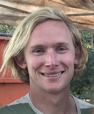
Johnny Davenport received his PhD in physics at University of California: Santa Cruz. He studied the electronic behavior of graphene and other two-dimensional (2D) materials in high magnetic fields. Specifically, Johnny uses tunneling spectroscopy to probe fractional quantum hall states that may be useful for quantum information processing, Johnny has expertise in fabricating and measuring nano-devices made of 2D materials. He received his BS in physics, math and chemistry from Sewanee: The University of the South and an MS in physics from UC Santa Cruz. Throughout graduate school, Johnny used graphene to teach condensed matter physics. Since 2016, he has worked with Professor Randy Peterson to develop an advanced lab focused on graphene isolation, fabrication, characterization and measurement.
Johnny Davenport, Dept. of Physics, U.C. Santa Cruz, 319A Walnut Ave, Santa Cruz, CA. 95060. Email : jodavenp@ucsc.edu. Phone: 415-419-6267.
 Eugene Donev does nanoplasmonics and nanophotonics research
and teaches introductory physics, advanced laboratory, optics and physics
seminar (capstone) courses in the Department of Physics and Astronomy at the
University of the South (Sewanee). After graduating from Sewanee with a BS
degree in physics and German, and earning MS and PhD degrees in physics from
Vanderbilt University, he received postdoctoral training at the University of
Kentucky, Brookhaven National Laboratory and the University of North Carolina
at Chapel Hill. Dr. Donev's teaching and research interests frequently
intersect as he incorporates elements of his work on the fabrication, optical
interrogation and numerical simulation of functional nanomaterials into
advanced laboratory projects for undergraduate students.
Please note that the Jonathan F. Reichert Foundation has established a grant program to help purchase apparatus used in Laboratory Immersions. Limitations and exclusions apply, but generally speaking the Foundation may support up to 50% of the cost of the required equipment.


